Category Archives: Uncategorized

Our Paper on “Low profile multi-layered invisibility carpet cloak using quantum dot core–shell nanoparticles”was accepted for publication in Scientific Reports.

Abstract

In this paper, a method to reduce the profile of layered carpet cloaks is proposed. We analytically prove and numerically demonstrate that using a Low Index Material (LIM), a material with a relative dielectric constant smaller than 1, in construction of carpet cloaks can remarkably reduce their profiles. Using the proposed technique, a carpet cloak consisting of alternating LIM and silicon layers is designed to provide invisibility at visible wavelengths. The designed cloak has a profile that is 2.3 times smaller than a carpet cloak without LIM layers. To realize low index materials at optical wavelengths, silver-coated CdSe/CdS quantum dots dispersed in a polymer host are used. Quantum dots are utilized to compensate the loss of Silver and to achieve a low index medium with neglectable loss. The designed low profile carpet cloak is numerically analyzed showing a good performance for a wide range of incident angles which is the advantage of the proposed structure in comparison with metasurface-based carpet cloaks which work only for a very narrow range of incident angles.


link:

https://www.nature.com/articles/s41598-023-30389-2

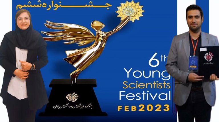
Congrats to Atefeh, my dear MSc student, for winning this prestigious award. Well done Atefe Shahsavari-Pour.


Congratulations to Mr. Mohammad-Hossein Badiei and Ms. Atefe Shahsavari pour, two students from the School of Electrical and Computer Engineering, University of Tehran for winning the first place in Mathematics and Computer Science at the 6th Young Scientists International Festival, held by Jamili Foundation to support the young generation of the world in five fields of basic science.
The festival was held in two sections, Startups groups and Ideators, and had a unique approach to coronavirus and artificial intelligence. Young scientists from around the world were invited to participate in the festival, which aimed to inspire and recognize the achievements of the next generation of scientists.
Mr. Badiei and Ms. Shahsavari-pour distinguished themselves from other participants in Mathematics and Computer Science, showcasing their knowledge, skills, and expertise in the field. Their achievement demonstrates the remarkable potential of young scientists and serves as an inspiration to others pursuing similar fields.
For more information:
https://lnkd.in/ehviDNca


Our Paper on “Developing a carpet cloak operating for a wide range of incident angles using a deep neural network and PSO algorithm”was accepted for publication in Scientific Reports.

Abstract

Designing invisibility cloaks has always been one of the most fascinating fields of research; in this regard, metasurface-based carpet cloaks have drawn researchers’ attention due to their inherent tenuousness, resulting in a lower loss and easier fabrication. However, their performances are dependent on the incident angle of the coming wave; as a result, designing a carpet cloak capable of rendering objects under it invisible for a wide range of angles requires advanced methods. In this paper, using the Particle Swarm Optimization (PSO) algorithm, along with a trained neural network, a metasurface-based carpet cloak is developed capable to operate for a wide range of incident angles. The deep neural network is trained and used in order to accelerate the process of calculation of reflection phases provided by different unit cell designs. The resultant carpet cloak is numerically analyzed, and its response is presented and discussed. Both near-field and far-field results show that the designed carpet cloak operates very well for all incident angles in the range of 0 to 65 degrees.

link:

https://www.nature.com/articles/s41598-023-27458-x

Our Paper on “Far-field sub-wavelength imaging”was accepted for publication in Optics Express.

Abstract

Due to the wave nature of light, the resolution achieved in conventional imaging systems is limited to around half of the wavelength. The reason behind this limitation, called diffraction limit, is that part of the information of the object carried by the evanescent waves scattered from an abject. Although retrieving information from propagating waves is not difficult in the far-field region, it is very challenging in the case of evanescent waves, which decay exponentially as travel and lose their power in the far-field region. In this paper, we design a high-order continuous dielectric metasurface to convert evanescent waves into propagating modes and subsequently to reconstruct super-resolution images in the far field. The designed metasurface is characterized and its performance for sub-wavelength imaging is verified using full wave numerical simulations. Simulation results show that the designed continuous high-order metasurface can convert a large group of evanescent waves into propagating ones. The designed metasurface is then used to reconstruct the image of objects with sub-wavelength features, and an image with the resolution of λ/5.5 is achieved.

link:

https://opg.optica.org/oe/fulltext.cfm?uri=oe-30-21-39025&id=509746

Our Paper on “Thermal insulator film with transparency to visible light”was accepted for publication in JOSA B.

Abstract

A method to develop an insulator window film which is able to filter thermal emission while transmitting the visible spectrum of sunlight is proposed. The proposed film is constructed from engineered metallic nano-spheres randomly distributed in SiO2SiO2, as a host medium. The performance of the designed film is investigated using both analytical models and numerical full-wave simulations. The analytical analysis shows that the thermal emission (the wavelengths in the range of 6–16 µm) is suppressed by more than 10 dB when going through the designed film, meaning that more than 90% of the thermal power is filtered by the film. This is while more than 50% of the visible light passes through the film. Similar results are obtained using numerical full-wave simulations. Moreover, to have a more comprehensive study on the ability of our method, the illuminance due to the insulator window film is calculated and compared with illuminance in different places. This comparison shows that the resultant illuminance in a typical room at the distance of 4 m from the designed window is in the range of illuminance required in a typical office room.

link:

https://opg.optica.org/josab/fulltext.cfm?uri=josab-39-10-2760&id=506490#

Our Paper on “Design and analysis of multi-layer silicon nanoparticle solar cells”was accepted for publication in Scientific Reports.

Abstract

We investigate the concept of nanoparticle-based solar cells composed of a silicon nanoparticle stack as a light trapping absorber for ultrathin photovoltaics. We study the potential of using these inherently nanotextured structures in enhancing the light absorption. For this, a detailed optical analysis is performed on dependency of the cell response to parameters such as the number of particle layers, lattice structure and angle of incidence; Optical response of these cells are then compared with the results in conventional silicon solar cells. Moreover, we propose various configurations to apply these submicron particles as a p–n junction solar cell. We also compute the electrical performance of selected configurations. In doing so, key issues including the effect of contact points between nanoparticles and impact of loss are addressed. In the end, we show how SiO2SiO2 nanoparticles on top of the cell structure can enhance the photocurrent. The appropriate range of SiO2SiO2 particle size is also obtained for the typical cell structures.


link:

https://www.nature.com/articles/s41598-022-17677-z
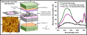
Our Paper on “A periodic perforated graphene in optical nanocavity absorbers”was accepted for publication in Materials Science and Engineering.

Abstract

Aperiodic perforated graphene layers were synthesized and used in fabrication of optical nanocavity absorbers. Chemical vapor deposition-grown graphene (Gr) layers were exposed to oxygen plasma etching to obtain the perforated graphene (pGr). The fabricated pGr/SiO2 (68 nm)/Ag (150 nm) nanocavity could present significant higher optical absorption, especially at around 530 nm wavelength region, as compared to a benchmark Gr/SiO2 (68 nm)/Ag (150 nm) sample. The effect of pore size of the pGr layer on the absorption property of the nanocavity has been studied by both experimental and numerical methods. The dependence of the absorption property of the nanocavity on the incident angles of unpolarized light and also the electrical/magnetical portion of transverse polarized light have been examined. The electrical interaction between the nanopores of the pGr and the incident light was found as the main reason for the absorption. The proposed graphene-based nanocavity resonator can further excite designing high efficient electromagnetic wave absorbers highly demanding two-dimensional coatings with effective optical absorption features.

link:

https://www.sciencedirect.com/science/article/abs/pii/S0921510721005110

Our Paper on “A Novel Plasmonic Bio-Sensor Operating Based on Optical Beam Steering”was accepted for publication in IEEE,Journal of Lightwave Technology.

Abstract

In this paper, a new architecture for developing plasmonic bio-sensors is proposed in which sensing is achieved through optical beam steering. The proposed structure consists of an array of nano-antennas that generate an outcoming optical beam whose direction varies when the material under test or its volume changes. This mechanism of sensing eliminates the requirement for complex instruments such as optical spectrum analyzers. For realization of the proposed bio-sensor, both 1-D and 2-D configurations for the nano-antenna array are designed and numerically studied. The full wave numerical simulation results show that the designed bio-sensor provides a very high sensitivity of 3333∘ per unit refractive index, and also the output light has an enough intensity to be observed by a naked eye. The final results show that although both versions have the same sensitivity, the 2-D structure can project the results with much higher intensity. It is also theoretically shown that the performance of the biosensor will be subject to the size of the array, and therefore, a practical large-scale version of the numerically studied structure would significantly outperform the simulated structure.

link:

https://opg.optica.org/jlt/abstract.cfm?uri=jlt-40-1-277

Our Paper on “Light trapping in thin film crystalline silicon solar cells”was accepted for publication in Optics & Laser Technology.

Abstract

In this paper, a new method is proposed to trap sunlight in the active layer of thin film solar cells. In the proposed technique, multi-scale photonic topological insulators (PTI) realized by photonic crystals, are integrated inside the active layer of a thin film solar cell in order to trap sunlight in the cell. The trapping is realized by excitation of edge states supported by the designed topological insulator. The performance of the proposed solar cell with the topological insulator inside is investigated through full wave numerical analysis. Numerical results show that the proposed method enhances the absorption of the solar spectrum inside the cell in a wide range of wavelengths, and also for different angles of incidence. The short circuit current provided by the proposed solar cell is numerically calculated illustrating a value of 27.72 mA/cm2 for a normally incident light which is 47% higher than a simple solar cell without topological insulator inside.

link:

https://www.sciencedirect.com/science/article/abs/pii/S0030399221005454